Silicon Genesis Enhances 3DIC Integration with Breakthrough in NanoCleave™ Ultra-Thin Layer Transfer Technology
NanoCleave™ enables transfer of 140nm ultra-thin silicon layers for cost-effective sustainable alternative to Temporary-Bond/Grind-Back/Layer-Release processes.
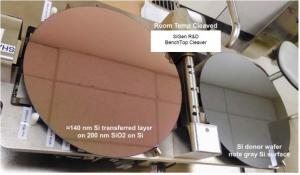
This innovative process enables the transfer of ultra-thin silicon layers, as thin as 140 nm (Figure 1), with outstanding thickness uniformity and smoothness, providing a cost-effective and sustainable alternative to traditional Temporary-Bond/Grind-Back/Layer-Release (TBGB) processes. NanoCleave™ unlocks unprecedented possibilities for integrating Three-Dimensional Integrated Circuits (3DIC).
The semiconductor industry is under increasing pressure to deliver higher performance devices while reducing costs and embracing sustainable practices. SiGen’s NanoCleave™ technology offers transformative solutions by eliminating the limitations of existing processes, such as stress-induced cracking, complex grinding steps, and layer thinning constraints. This proprietary room-temperature cleaving technology enhances precision, efficiency, and environmental sustainability.
Key Features of NanoCleave™
1. Ultra-Thin Layer Transfer: NanoCleave™ achieves silicon layer thicknesses of 140 nm and less on 300 mm wafers with remarkable layer thickness uniformity and smoothness as well as layer thicknesses up to 2 µm on 200mm and 300mm wafers. By removing the need for complex grinding or polishing steps, it provides manufacturers with a simplified and cost-efficient process for advanced applications in 3DICs.
2. Room-Temperature Operation: Unlike competing technologies, which require higher temperatures—such as Ion-cut methods operating above 300°C or laser techniques involving pulsed exposures to 800°C, NanoCleave™ operates at room temperature following bond annealing at 275°C. This reduces thermal stress, ensuring device integrity and lowering overall manufacturing risks.
3. Sustainability and Cost Savings: The NanoCleave™ process supports donor wafer recovery using a single-step Epitaxial Smoothing/Gas Phase Epitaxial Regrowth technology developed in partnership with Applied Materials (AMAT). Epitaxial layer crystalline quality is superior compared to poly-crystalline deposition by CVD processes. This recovery process minimizes material waste and contributes to the industry's drive toward greener, more sustainable manufacturing practices.
4. TBGB Process Replacement: NanoCleave™ offers a superior alternative to the TBGB process by addressing critical challenges:
• CMP Stress Cracking: Avoids dry-grinding and chemical-mechanical polishing, which often leads to micro-cracks in thin silicon layers.
• Thinning Limitations: Achieves consistent thinning to less than 2 µm, a level unattainable by mechanical thinning methods that struggle below 20 µm.
5. Back-End-of-Line (BEOL) Optimization: SiGen’s solution supports fine-line metal geometries for device interconnection, enabling efficient BEOL processing. This innovation surpasses the limitations of the traditional 10:1 aspect ratio through-silicon vias (TSVs) for example in 100 µm thick layers, improving signal bandwidth by an order of magnitude and reducing power consumption in advanced semiconductor designs.
Competing Technologies and Their Limitations
1. Ion-cut Technology: While Ion-cut is an alternative; it depends on higher doses of hydrogen ion implantation and annealing temperatures exceeding 300°C. These requirements pose significant thermal challenges, particularly for sensitive devices and higher cost of ownership. NanoCleave™ bypasses these obstacles, using lower hydrogen implant doses, cleaving at 25°C and preserving device integrity.
2. IR Laser Techniques: Laser-based methods require deposition of additional layers on carrier wafers, such as absorber and reflective coatings, to shield devices from thermal exposure up to 800°C. These added steps complicate workflows and raise costs. NanoCleave™ eliminates the need for these layers, simplifying the manufacturing process while reducing potential damage to devices.
Advantages of NanocleaveTM for 3DIC Integration
SiGen’s NanoCleave™ technology represents a paradigm shift in 3DIC manufacturing, addressing critical challenges and enabling next-generation semiconductor design:
1. Thermal Management: Ultra-thin silicon layers with integrated cooling channels improve heat dissipation within chip stacks, reducing hotspots and enhancing performance.
2. Shortened Interconnect Distances: By enabling thinner layer vertical stacking, NanoCleave™ facilitates shorter high-bandwidth interconnects, improving signal speed and energy efficiency.
3. Enhanced Reliability: The uniformity and smoothness of transferred layers contribute to better device yields and overall product reliability.
Applications in Semiconductor Packaging
NanoCleave™ supports diverse applications in semiconductor packaging, particularly in producing advanced 3DIC architectures. It enables heterogeneous integration of logic, memory, and photonics, crucial for the development of next-generation devices in artificial intelligence (AI), high-performance computing (HPC), and telecommunications.
Commitment to Sustainability
SiGen’s NanoCleave™ aligns with global efforts to reduce the environmental impact of semiconductor manufacturing. By enabling donor wafer recovery and reducing material waste, the process provides a greener alternative for high-performance manufacturing.
Positioning NanoCleave™ for the Future
As semiconductor demands grow, SiGen’s NanoCleave™ technology is well-positioned to support emerging trends. Its cost efficiency, compatibility with cutting-edge manufacturing techniques, and environmental advantages make it a cornerstone of the future of 3DIC integration.
About Silicon Genesis
Silicon Genesis is a leading provider of engineered substrate process technology and equipment. SiGen’s technology is used for production of Silicon-on-Insulator (SOI) semiconductor wafers and 3DIC stacks of CMOS device layers for high performance applications. Founded in 1997, SiGen is headquartered in Fremont, California. For more information, visit www.sigen.com for the complete SiGen NanoTec offerings of layer transfer process, equipment technology and services.
Ted Fong
Silicon Genesis Corporation
+1 408-228-5885
tfong@sigen.com
Distribution channels: Electronics Industry, IT Industry, Manufacturing, Science, Technology
Legal Disclaimer:
EIN Presswire provides this news content "as is" without warranty of any kind. We do not accept any responsibility or liability for the accuracy, content, images, videos, licenses, completeness, legality, or reliability of the information contained in this article. If you have any complaints or copyright issues related to this article, kindly contact the author above.
Submit your press release
