
Australia’s place in the semiconductor world: The opportunities for Australia in the semiconductor industry
As our Australia’s place in the semiconductor world editorial series draws to a close, Steven Duvall and Glenn Downey provide the final part of their four-part feature. Here they propose steps to help build the semiconductor industry in Australia
1) Introduction
This article concludes our four-part feature on semiconductors, continuing the themes from the three previous articles, focusing on the case for semiconductor manufacturing in Australia.
Part 1 provided background on semiconductors aimed at an audience with little or no background on the subject. A high-level overview of fundamental properties of semiconductors led to a discussion of the industry and the impacts it has had.

Part 2 examined the impacts of recent shortages of semiconductor components, the vulnerabilities they have revealed in global supply chains and the responses they have prompted by countries around the world.
Part 3 examined the significance of semiconductors for Australia and considered some of the challenges faced by Australia as it seeks to grow its semiconductor industry.
In Part 4, we propose steps to help build the semiconductor industry in Australia.

2) Growing Australia’s semiconductor industry
In the previous three parts of this series, we discussed the growing strategic importance of semiconductors globally, efforts by countries around the world to increase their self-sufficiency in semiconductors, and the importance for Australia to grow its participation in the semiconductor industry.
We framed the importance for Australia in terms of two mutually supporting imperatives:
- A strategic imperative to provide trusted domestic sources of (some) critical components; and
- An economic imperative to build and retain knowledge and skills and drive economic growth.
This led us to two corresponding, mutually supporting objectives:
- To establish domestic sources of critical semiconductor components and
- To establish leadership in select semiconductor market segments that are both relevant to Australia and offer global market opportunities.
In this final part to our series, we consider how Australia can achieve these objectives.
In considering how to achieve these objectives, we must recognise that Australia cannot do everything. The complexity of semiconductor supply chains, the vast array of different products and technologies, and the huge base of intellectual property mean that we will need to carefully choose the areas in which to focus. We also need to appreciate that it will take time to achieve these objectives. Fab construction, technology development and product development and qualification all take years to complete.
3) Where in the supply chain?
Although we see opportunities throughout the supply chain, as discussed in Part 3, we think it is essential for Australia to grow its capabilities in semiconductor product development and manufacturing. Indeed, achieving the two objectives mentioned above requires both domestic product development and manufacturing.
By “product development,” we mean all steps involved in taking a semiconductor product from concept into production, including specification, design, verification, validation and qualification.
By “manufacturing,” we mean most stages of manufacturing described in Part 1, including epitaxy manufacturing, chip fabrication, dicing and assembly. We include only epitaxy from the “wafer manufacturing” stage from Part 1 as epitaxy is critical to product leadership in emerging and fast-growing segments of the semiconductor industry.
Achieving Objective 1 inherently requires onshore manufacturing.
Achieving Objective 2 inherently requires product leadership in the selected market segments through technology leadership, design leadership or, ideally, both, as discussed in Part 3. Access to and control of manufacturing, say through onshore manufacturing, enhances the ability to achieve technology leadership. The strategic alternative to product leadership of competing based on cost does not fit well with Australia’s global positioning.
Importantly, achieving leadership in any products will require more than product development and manufacturing capabilities. It will require strong capabilities in commercialisation, including the choice of markets, timing, and commercialisation execution with developed products.
To be clear, onshore product manufacturing will not eliminate reliance on overseas sources. As shown in Figure 1, product development and manufacturing require inputs, including design and development tools, equipment and materials, most of which will be sourced from overseas.
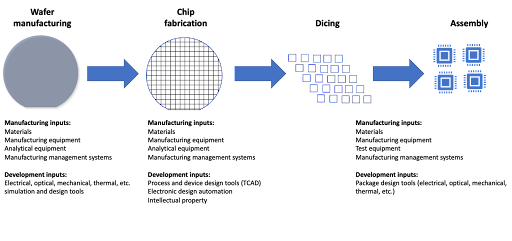 Figure 1 Source: Based on R. Schafer, J. Buchlater, Semiconductors: Technology and Market Primer 10.0, Oppenheimer & Co, Inc. 2017
While an open trade and benign geopolitical environment would keep all our sourcing options (and geographic market destinations for product) available, the near-term future for Australia is to add clear and distinct value to ‘friend-shoring’ supply-chain initiatives.
4) What technologies?
For the sake of this discussion, we impose some order on the very broad and diverse range of semiconductor technologies by grouping them into three technology domains: advanced silicon technologies, mature silicon technologies and non-silicon technologies.
By advanced silicon technologies we mean the most advanced semiconductor manufacturing processes, say, 40nm and beyond. They deliver the smallest transistors, the highest levels of integration and the highest performance in highly integrated logic products, such as microprocessors and graphics processors. The industry leaders, TSMC, Samsung and Intel, are at the forefront of advanced silicon manufacturing, but other foundries offer advanced silicon technologies, including GlobalFoundries and UMC.
Advanced silicon technologies are effectively out of reach for manufacturing in Australia, short of being able to attract an established manufacturer to invest in constructing an advanced silicon fFab within the country. An Australian company seeking to build and operate an advanced silicon fab would face enormous barriers including cost, lack of sufficient skills and expertise, and lack of the required ecosystem in Australia. Perhaps most importantly, such a company would face an enormous barrier in the huge base of know-how developed progressively by the technology leaders over many years and many generations of technology and products.
To provide current context, Japan is seeking to re-establish semiconductor technology leadership through a consortium of eight firms and an initial investment of ¥7.3 billion with a likely cost of ¥5 trillion (about AU$53 billion).
By mature silicon technologies we mean the wonderfully wide and diverse range of silicon-based semiconductor manufacturing technologies, including mature node silicon CMOS and special purpose technologies for power and RF switches. Mature silicon technologies represent the bulk of the installed base of semiconductor manufacturing capacity. Most of the chip supply shortages of the past few years were due to lack of capacity on mature silicon manufacturing process lines.
We see opportunities for Australia in mature silicon technologies, but building a fab is not the right starting point. Rather, we would seek to build product leadership through design on commercially available processes available at overseas foundries, many of which are highly depreciated and, so, relatively inexpensive.
In parallel, we would look for ways to extend product leadership through innovations in technology, perhaps in new devices, new materials integrated into silicon, or new ways to manipulate and combine active silicon layers. We would seek to prove these technology innovations in existing domestic facilities (such as ANFF). We would only consider building a fab once the technology had been proven and product leadership established. We would consider starting the fab with a mature node silicon CMOS technology licensed from overseas, which is not an unfamiliar approach given that is how TSMC started.
By non-silicon technologies we mean all remaining semiconductor technologies, most of which are based on compound semiconductors, such as gallium arsenide, indium phosphide, gallium nitride, silicon carbide and diamond. As discussed in Part 1, these technologies are used when the properties of silicon are not “good enough” for the application. Some of the fastest growing segments of the semiconductor industry at present are based on compound semiconductors.
We see significant opportunities for Australia to build on its foundation of compound semiconductor capability in universities and industry to (relatively) rapidly establish a domestic source of critical semiconductor components for Defence (objective 1) and accelerate progress toward commercial leadership in relevant sectors of the industry (objective 2). Central to this effort would be the establishment of a compound semiconductor fab focused on Australian needs and opportunities. The fab would support both epitaxy and device manufacturing. Indeed, epitaxy design is intimately related to product design in compound semiconductors so access to epitaxy and device manufacturing capabilities are essential.
Domestic manufacturing would accelerate product development by reducing cycle times and would facilitate technology and product innovation, enabling product leadership.
Product leadership in compound semiconductor devices can be achieved without the most advanced semiconductor processing equipment. For example, photolithography capabilities equivalent to 20-year-old silicon CMOS technologies are sufficient for most compound semiconductor products of potential interest.
A compound semiconductor fab in Australia would not face costs comparable to advanced silicon CMOS fabs. The capacity, and hence, the cost of a compound semiconductor facility can be easily scaled up or down. Based on prior analysis, we expect that an investment of between $50 million and $100 million would be sufficient to build a compound semiconductor facility that would meet the requirements of Australian Defence for certain critical components (objective 1).
In addition, each of the main value chain steps in the compound semiconductor market remain relatively fluid and dynamic – the industry structure has not yet fully coalesced and determined clear market leaders with impenetrable moats. There remains a clear window of opportunity. We acknowledge that it is still a bet to introduce extra fab ‘supply’ onto the market at a time when other countries and companies have announced their own compound semiconductor fab commitments, but to the extent an Australian fab is underwritten by our own strategic needs, product for our own market use and advances the cause of developing Australian product leadership for global markets, the case becomes much more compelling. We can ‘buy’ a valued seat in the friend-shoring supply-chain.
We advocate an approach in which manufacturing and product development capability are grown progressively and in tandem, starting with the investment in compound semiconductor manufacturing capability mentioned in the previous paragraph. Additional manufacturing capacity would be established as demand and manufacturing know-how developed.
5) What products?
We see significant opportunities for compound semiconductors in three of the fastest growing and most strategic sectors of the semiconductor industry:
- Power (high voltage and current) applications, including rail traction, electric vehicles and power distribution for the ‘new energy grid’ transition,
- Wireless (RF, mm-wave and microwave) applications, including 5G and 6G for mobile phones, radar for civilian and military applications, and satellite communications, and
- Photonic (light emission and detection) applications in sensing, analytics and disinfection and purification.
We see wireless as the best near-term product opportunity for Australia based on the country’s long history in this field and existing domestic capabilities and industrial interest in relevant circuit and module design. It also aligns with strategic needs identified by Australian Defence and could potentially serve the needs of domestic systems integrators.
So, to draw the connection between product and manufacturing, we advocate that the compound semiconductor manufacturing facility proposed in the previous section focus initially on the requirements of fabricating devices for wireless applications.
6) Conclusion
We believe that the strategic and economic imperatives for Australia to develop its domestic semiconductor industry can be best satisfied by progressively growing product development and manufacturing capabilities. We see compound semiconductors as the best near-term opportunity and advocate establishing a moderate-sized compound semiconductor manufacturing facility focussed on wireless devices as the right step in this direction.
Picture: credit www.great.gov.uk
Dr. Steven Duvall has been in the semiconductor industry for nearly 40 years since completing his PhD at Stanford University in 1983. He spent 18 years with Intel in California driving corporate initiatives in design for manufacturability and six years with Intel in Australia supporting Intel Capital globally with technical and commercial due diligence of entrepreneurial companies. He spent 14 years with Silanna Semiconductor, an Australian developer and manufacturer of advanced semiconductor components, where he was the Chief Technology and General Manager of Ultraviolet Products.
Glenn Downey is Executive Director of The Maltby Group. Glenn was the primary author of the NSW Office of the Chief Scientist and Engineer’s ‘Australian Semiconductor Sector Report
(2020). Glenn co-founded and led Sydney based OFDM cable modem technology developer Aurora Communications Limited through till its acquisition by ADC Telecommunications, led the investment and commercialisation activities for Redfern Photonics, the commercialising vehicle for the Australian Photonics CRC, and was Commercialisation Director at NICTA prior to its merger with CSIRO.
@AuManufacturing and AUS-Semiconductor-Community’s editorial series, Australia’s place in the semiconductor world, is brought to you with the support of ANFF.

More in this section


@aumanufacturing Sections
Analysis and Commentary Awards Defence Manufacturing News Podcast Technology Videos